Plating of electronics substrate and devices for microelectronics
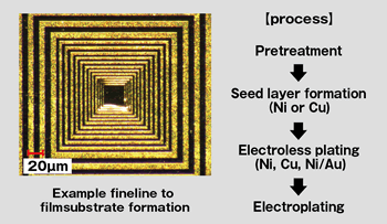
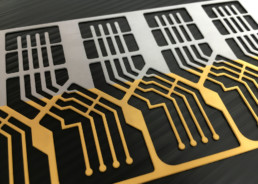
Electroless Au plating for fineline circuit on PC board
(L/S = 30/30µm)
Electroless Ni/Pd/Au plating for micro-circuit
Excellent soldering, wirebondability. 3layers plating:Ni/Pd/Au is improved surface mounting reliability.
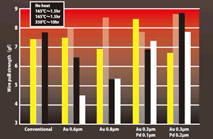
Au Wire pull test
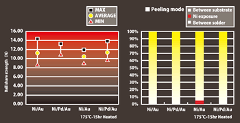
Ball share test
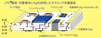
Au Plating for LTCC substrate
Electroless plating process for LTCC substrate silver electrode
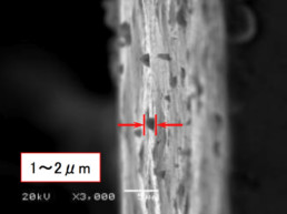
Wire pull strength on thicktype electroless Au plating film
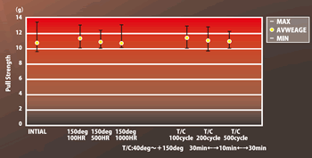
Electrode: Electroless plating on Ag/Pt
Plating thickness: Ni3μm Au0.4μm N=50
Au wire: 30μmφ Bonder: Kaijo118CH (Full auto type)
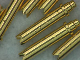
Gold plating for electroless wire bonding for semiconductor wafers
In recent years, while UBM formation (Under Bump Metal) by electroless plating on semiconductor wafer mounting pad electrodes has attracted attention, we have cultivated for many years, utilizing the gold plating technology for printed circuit boards used in SMD, etc., it is possible to process electroless gold plating for stable wire bonding.
Even wafers with a mixture of SR and polyimides can be selectively bonded gold plating on the pad.
| Plating Process | Plating Thickness | Wafer Size | Wafer Thickness | Pad | Pad Size |
| ENIG (Eletroless Ni/F-Au) | Ni:0.5~10um Pd:0.02~0.8um Au:0.02~0.8um | Small pieces ~8inch *10 inches can be prototyped | 300um~2mm ※300um or less Wafer reinforced by tape as needed | Al | φ10um~ Plating support possible |
| ENIGAG (Electroless Ni/Thick-Au) | Al-Si | ||||
| ENEPIG (Electroless Ni/Pd/F-Au) | Al-Si-Cu | ||||
| ENEPIGAG (Electroless Ni/Pd/Thick Au) | Al-Cu | ||||
| Cu |
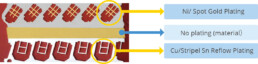
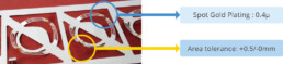
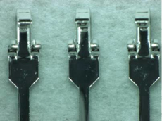
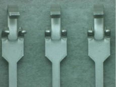
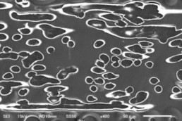
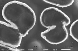
Micro spot plating for micro connector
Spot plating is plated with technology only where necessary.
Can significantly reduce the amount of use Au.
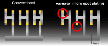
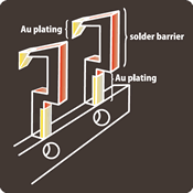
Material: Cu alloyMaterial Thicness: 0.08mm~Material width: ~20mmPlathing thicness: Ni 1μm~ Au0.1~0.5μmSolder Barrier area: 0.3mm~Method of forming a Solder Barrier : Lazer or special masking
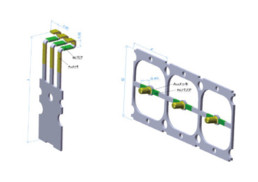
Example of Spot Plating
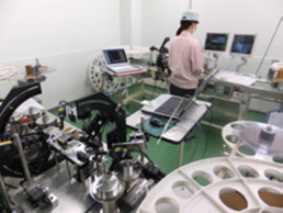
Visual Inspection System by in-house production
Reel to reel plating for presses devices for automotive applications
| Transport | By vertical transport, both single-tie bar and center carrier are possible. |
| Product shape | Materials, primary pressed both possible |
| The material amplitude | tandard Max100mmW *Consultation for more cases |
| Material thickness | Standard Max0.8mmt *Consultation for no more |
| Others | Consultation on mixed specifications of stripe and spot plating, stripe plating (±0.1 mm), etc. |
Four color plating
Reflow tin plating with each different thickness
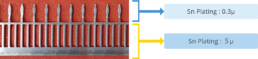
Spot plating
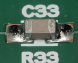
Sn reflow plating for automotive press-fit terminals

The temperature profile of the reflow is checked by the initial condition setting, and the pure tin thickness and the diffusion layer thickness are controlled. If necessary, we perform cross-sectional observation by CP and IM to ensure the plating layer structure.
Pb free plating
Reflow tin plating
Tin plating is used as an alternative to leadcontaining solder plating. It is necessary to take a measure for whisker. Internal stress of crystal particles which causes whiker can be eased by reflowing process. We produce reflow tin plating for connector in volume.
Before reflow
After reflow
Surface of reflow tin
Before reflow

After reflow
Before reflow

After reflow
Zero-cross time (second)
| After plating | PCT: 5hrs | PCT: 16hrs | ||||
| Before reflow | After reflow | Before reflow | After reflow | Before reflow | After reflow | |
| 1 | 0.33 | 0.80 | 0.47 | 0.70 | 0.58 | 1.08 |
| 2 | 0.43 | 0.70 | 0.42 | 0.80 | 0.51 | 1.36 |
| 3 | 0.32 | 0.69 | 0.40 | 0.93 | 0.48 | 1.50 |
| 4 | 0.32 | 0.71 | 0.50 | 0.95 | 0.30 | 1.04 |
| 5 | 0.35 | 0.44 | 0.63 | 1.16 | 0.43 | 1.48 |
| AVE. | 0.35 | 0.67 | 0.48 | 0.91 | 0.46 | 1.29 |
| MAX. | 0.43 | 1.80 | 0.63 | 1.16 | 0.58 | 1.50 |
| Min. | 0.32 | 0.44 | 0.40 | 0.70 | 0.30 | 1.04 |
| STD. | 0.05 | 0.13 | 0.09 | 0.17 | 0.10 | 0.22 |
Measurement: SWET-2000 / Sn-3Ag-0.5Cu Solder / Rosin flux
PCT: 121℃-100℃RH
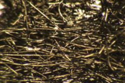
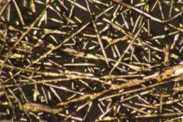
Reflow tin whiskers
Cu/Sn 1μm
46 days later
Non-reflow
After reflow
4 months later
Non-reflow
After reflow
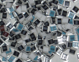
Barrel Plating
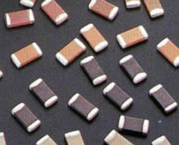
| Products | A | Chip resistor, Chip capacitor, Chip inductor, Chip filter, SMD products by chip type |
| B | Small stamping parts | |
| Size | A | min 1.0mm × 0.5mm ~ |
| B | Pin: min ø0.5mm × 2mm ~ Plate: min 2.0mm × 1.5mm ~ | |
| Plating Thickness | A | Electrolytic Ni, Sn or Au |
| B | Electroless Ni, Electro Ni / Electro Au, Electro Ni / Electro Sn, Electro Ni / Electro Ag, Electro Cu |
A) Possible to plate various chip size devices with flexible treatment.
B) Possible to plating small parts with various kind of plating.
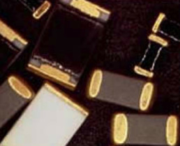
Gold plating for small connector parts
Tin plating to chip device
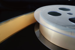
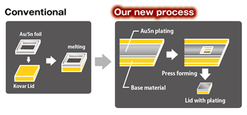
Plating on Metal foil
Continuous Ni and Au plating are possible for Cu, stainless steel foil material with the thinnest 10μm thick. (Maximum width 160mm)
It can be used as a reinforcing substrate for battery materials and flexible substrates.
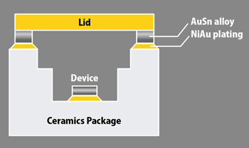
It is possible to form wax materials with gold tin, silver tin, and silver copper by plating method to 30μm thick kovar material.
It is used as a sealing material such as ceramic packages.
| Material Thickness | Plating | Plating Thickness | |
| Kovar | 10μm | Au80/Sn20 | 4~20μm |
| Ag/Sn5 | ~200μm | ||
| Ag/Cu | 4μm~ | ||
| SUS・Cu | Ni・Au | 1μm~ | |
| Film with Cu | 20μm~ | Ni/Au | 1μm/0.1μm~ |
Gold Tin Alloys by plating forming for Brazing assembly
Can form the plating material is used in brazing electronic packaging devices.
80Au/20Sn alloys by plating forming.
Comparison of plating with rolling foil
| plating | traditinal | |
| Oxdation | ○ | ○ |
| Base material selection | ○ | △ |
| Out gas | ○ | ○ |
| wettability | ○ | ○ |
| Thicness control | ◎ | △ |
| cost | ○ | △ |
| Ratio control | ○ | △ |
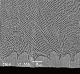
Molten state of plating Au80/Sn20
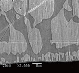
Molten state of Traditional brazing
New technology of plating for microelectronics
Etching free plating without using roughned process
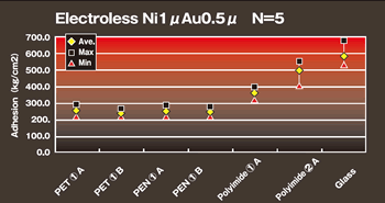
Direct plating of organic film material
Traditionally, when film formation to maintain smooth as glass and plastic, been using dry process is expensive.
Maintaining surface smoothness of the material, can form a solid film by this new plating process.
Maintain the smoothness of nanoscale.
Without using a dry process, polyimide,glass,PET, PEN ,PPA, LCP, Polycarbonate plating can be formed into high performance and lowcost.
Can also ITO electrode plating thicktype electroless Au.
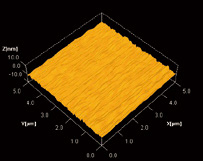
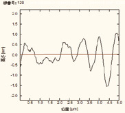
Direct plating on glass
Usually, direct plating to glass strongly roughs the glass surface with hydrofluoric acid, etc., but in our development process, it is possible to form a plating film with mirror gloss by adopting a unique pretreatment that hardly devastates the material and a unique electroless plating with high uniformity.
Electroless Cu plating
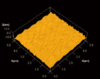
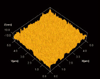
Appearance surface roughness after platingOur pretreatment, which hardly devastates the material, allows the surface roughness of the nano-order to form a high-adhesion plating film.
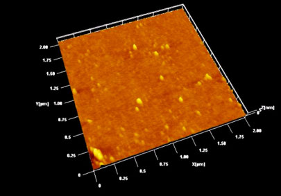
Before Pre-treatment Ra: 0.5nm
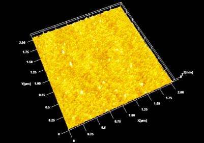
After pretreatment Ra: 1nm
Zinc-free plating on aluminum
Usually, aluminum materials are highly solubility in acids and alkalis, and it is common to chemically perform zinc substitution (zinc treatment) and perform plating processing.
This technology is capable of plating directly into aluminum materials without zinc replacement treatment.
As a result, the process is shortened, and the partial plating method can be easily performed.
Process
Preprocessing
↓
Material etching
↓
Au Strike Plating
↓
Bondable Au plating
Example of direct gold plating for aluminum lead frame
Material: A1020P.
Au plating thickness: 1μm (stripe plating)
Plating to non-woven fabric
It is a technology to uniformly coat various plating coatings to fibers such as non-woven fabric.
Material: Poliolephin
Ni plating thickness: 0.1μm~
Material: Polyester
Ni plating thickness: 0.1μm~
FIB SIM
Material: PP weaving.
Sn plating thickness: 0.5μm~
FIB SIM
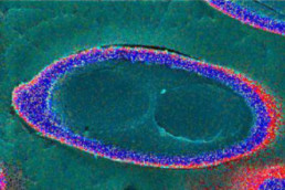
Cross-section EDS mapping
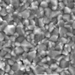
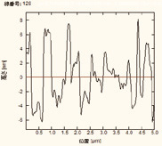
Roughed Ni plating
Nickel plating with an increased surface area by roughing the plating film can be produced for applications such as improving adhesion to resins. The entire surface is uneven and the Rz is over 2.0 μm.
FE-SEM secondary electron image (40° tilt)
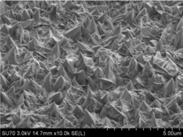
Example of coarsened nickel plating
Material: Copper plate
Ni plating thickness: 5.0μm~
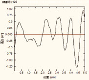
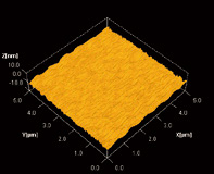
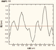
Unevenness measurement (laser microscope)
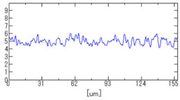
Roughness measurement results
Ra 0.31um
Rz 2.04um
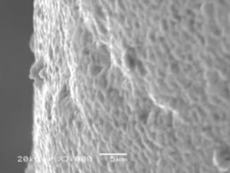
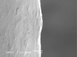
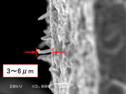
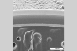
Direct plating for titanium and SUS
Gold plating and nickel plating are possible directly on titanium, which is represented by difficult-to-plating materials. There is no defect between the material and the plating, and the adhesion is good. In addition, copper plating with good direct adhesion on SUS also possible.
FIB SIM image
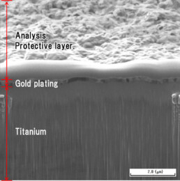
Example of direct gold plating for titanium
Material: Titanium
Au plating thickness: 0.2μm~
FIB SIM image
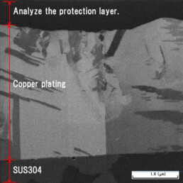
Example of direct copper plating of stainless steel
Material: SUS304
Cu plating thickness: 3.0μm~
Electroless plating on ITO electrade
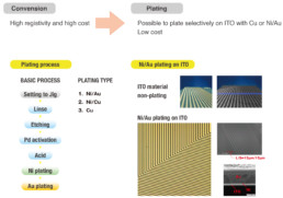
Roughness if surface on ITO and glass substrate after etching
ITO: Before etching
Ra: 0.65nm Rz: 3.62nm
ITO: After etching
Ra: 2.78nm Rz: 14.37nm
Glass: Before etching
Ra: 0.35nm Rz: 1.84nm
Glass: After etching
Ra: 0.42nm Rz: 2.25nm
By etching ITO selectively, the surface of glass has not changed while the ITO surface gets four times rough.